HBTs: Heterojunction Bipolar Transistors
Single and Double Heterostructure Bipolar Transistors (InP/GaInAs)
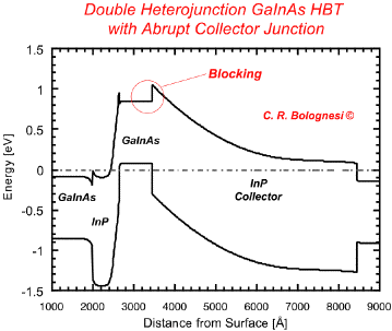
InP/GaInAs HBTs are of central importance to the development of modern lightwave communication systems such as 40 Gb/s optical communication systems because they are compatible for integration with 1.3-1.5µm optoelectronic components such as lasers and photodetectors. At present only a few companies like Hughes, TRW, and Lucent provide commercial products based on InP HBTs. InP/GaInAs HBTs are the fastest bipolar transistors ever fabricated, but they present a number of complications related to the low breakdown voltages achievable in the narrow bandgap GaInAs (0.75eV) collectors. Double heterostructure HBTs with a wide bandgap InP or InAlAs collector permit marked improvements in breakdown voltages but tend to cause a blocking effect of electrons flowing through the base and into the collector. The blocking effects can be alleviated by grading the collector/base junction alloy composition, and various schemes have been developed (binary or chirped superlattice grading; or analog compositional grading) but all are sensitive to the exact details of the grading scheme.
The figure on top shows the equilibrium energy band diagram for an abrupt junction double heterostructure InP/GaInAs bipolar transistor. Complex grading schemes are required to alleviate the collector current blocking effect.
We are also investigating InP/GaInAs DHBTs with an InP collector because InP displays higher peak and saturated electron drift velocities, a high breakdown field of ~480 MV/cm, and a high thermal conductivity which allows an efficient heat dissipation in power HBTs operated at high voltages.
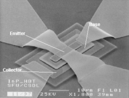
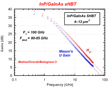
A fully self-aligned wet etch process was developed with evaporated (rather than electroplated) airbridge interconnects. Relatively large area emitter devices (4x12 µm2) have resulted in current gain cutoff frequencies as high as fT=105GHz with a maximum oscillation frequency fmax=85GHz. Scaling of the emitter width to 1µm will result in fmax values beyond 200GHz.
Figure on the left shown a Scanning Electron Microscope image of a 100GHz fully self-aligned InP/GaInAs heterostructure bipolar transistor with a 750Å base and a 7000Å collector. The emitter is on top. Note the evaporated airbridge interconnects. The process is carried out with wet etches only: the resulting surfaces are damage-free, and large BVceo voltages of 11-12V are achieved.
Double Heterostructure Bipolar Transistors (InP/GaAsSb/InP)
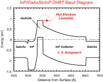
We have developed InP/GaAsSb/InP DHBTs that overcome the collector blocking effect described above by engineering MOCVD-grown DHBTs in which the GaAsSb p-base conduction band edge sits above the InP conduction band edge: instead of being slowed down by a blocking/opposing field due a to a chemical potential gradient, electrons reaching the base/collector junction benefit from a ballistic injection launching ramp that injects them into the InP collector with a high velocity: it is the total integrated velocity across the collector layer that determines the collector transit time, and we believe the ballistic launcher will prove very helpful in the realization of high speed InP based DHBTs. Our first public report of InP/GaAsSb/InP DHBTs was given at the 1998 IEEE Device Research Conference held June 22-24, 1998 in Charlottesville, VA.
The figure on the upper left shows the equilibrium energy band diagram for an abrupt junction double heterostructure InP/GaAsSb/InP bipolar transistors. Note the ballistic electron launcher at the abrupt base-collector junction. The conduction band discontinuity at the InP/GaAsSb interface was determined by sophisticated high-resolution FTIR photoluminescence measurements of the type II recombination at the interface. The conduction band offset is equal to 0.18eV.
The figure on the left (click for a larger version) shows room temperature I-V characteristics for a small area InP/GaAsSb/InP DHBTs. BVceo = 6-8V for a 1500Å InP collector layer. The knee voltage is smaller than 0.2V, a great advantage over the usual 0.6V of conventional GaAs MESFETs/HEMTs and HBTs. The collector offset voltage is 12-15mV because of the complete symmetry of the E/B and B/C heterojunctions.
InP/GaAsSb DHBTs have previously been explored by two other groups (Bellcore / Rockwell), but SFU was the first to demonstrate very nearly ideal Gummel characteristics and record collector Vce offset voltages as low as (12-15mV). The base and collector current ideality factors nb and nc are equal to 1.0 in both normal and reverse operation. Cutoff frequencies as high as 75GHz were also achieved in non-optimized structures. We attribute the improved performance of our devices to the careful selection of the growth conditions by cross-correlating the results of AFM, XRD, FTIR-PL, and device measurements.
Such low offset voltages are very attractive for wireless communication systems because there is an urgent need to develop highly efficient low-voltage power amplifiers: in 1998, wireless handset systems have begun a transition to 3.6V supply voltages (with either a 3-cell NiCd or NiMH or a single cell Li+ battery configuration). Note that in the early 1990's the supply voltage for wireless phones was 7.2V (achieved with 6 NiCd cells)-- so many batteries made the handsets bulky and heavy, and the high power dissipation affected the component lifetime. The drive to low-voltage and high amplifier efficiencies is of course fueled by the consumer demand for small handyphones with long talk-times between recharge cycles. As a 3.6V battery pack discharges, its voltage can drop as low as 2.7-3.0V: the power amplifier must continue to perform well as the supply voltage drops toward its end voltage (when the battery is completely discharged).
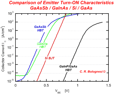
The potential advantages of InP-based HBTs, and particularly those of InP/GaAsSb DHBTs, for wireless handset applications are made very clear by comparing the collector current turn-on characteristics of bipolar transistors for various material systems.
The figure on the left shows measured collector current densities in A/cm2 as a function of Vbe for InP/GaAsSb, InP/GaInAs, Si, and GaInP/GaAs transistors. Note how the voltage required for a certain collector current is much smaller in InP-based HBTs than for GaAs HBTs: this is largely a consequence of the smaller base material energy gaps. Base energy gaps: GaAs=1.42eV; Si=1.12eV; GaInAs=0.75eV; and GaAsSb=0.72eV. The saturation at high currents is due to probe and contact series resistance effects.
Check Download this (PDF, 555 KB) article from the Agilent Measurement Journal - 2007 Issue for a brief overlook on the History of InP/GaAsSb DHBTs.