Indium Phosphide (InP) HEMTs
Thanks to the excellent transport properties of the InP/GaInAs material system, InP HEMTs (High Electron Mobility Transistors) offer the best performance for low-noise and high-frequency applications (for example, in extremely low noise amplifiers). Typical applications can be found in the fields of deepspace communications and radio astronomy, which impose stringent demands on the signal amplification and therefore require cryogenic operation of the transistors at temperatures of ~10K.
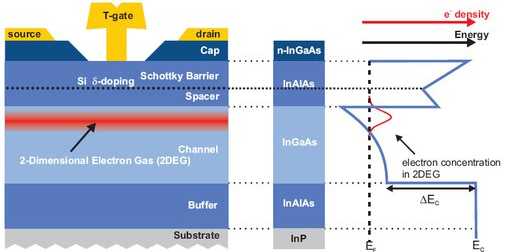
Taking advantage of the fact that the 2DEG offers exceptional high carrier mobilities compared to bulk material, a typical InP-HEMT has the following layer structure:
- Silicon δ-doping layer: Highly doped layer with only few atomic layers thickness. Located between the Schottky-Barrier and Spacer layer. Acting as a donor of charge carriers, i.e. it provides electrons to the channel. Since electrons tend to occupy the lowest allowed energy state, they drain into the potential well and form the confined 2DEG in the channel. A high δ-doping level provides high electron densities in the channel and therefore results in high transconductances, current densities and
cut-off frequencies. - The Spacer layer assures the separation between the electrons and their positively charged Si-donors, reducing impurity scattering and hence enhancing electron mobility.
- Cap: A highly n-doped cap layer helps minimize the contact resistance of the source and drain contacts. The cap also provides protection from oxidation for the sensitive InAlAs layer beneath.
- Schottky-Barrier: The Schottky-Barrier layer, in contrast to the Ohmic source and drain contacts, provides a so-called Schottky contact between gate-metal and semiconductor material with a rectifying characteristic. It prevents large currents from flowing trough the gate and limits tunneling to the channel.
Channel properties have a major impact on the device performance. This is why InGaAs, with its excellent electron mobility properties at room and cryogenic temperatures, is the material of choice.
The special T-shape of the gate helps minimize the gate resistance by enlarging the cross section while maintaining a small foot-print and thus a small gate length.
Applications
InP-HEMTs show excellent noise and gain performances at microwave frequencies. At cryogenic temperatures, these properties improve further. This predestines InP-HEMTs for receiver systems, which have the most stringent requirements for low noise and high sensitivity. ETH “in-house” developed and processed HEMTs are being deployed in the missions of external page ESA (European Space Agency) and the space observatory external page IRAM (Institut de Radio Astronomie Millimetrique). ETH has contributed to several projects involving cryogenically (~10K) cooled two- and three-stage low noise amplifiers (LNA).

