Lab
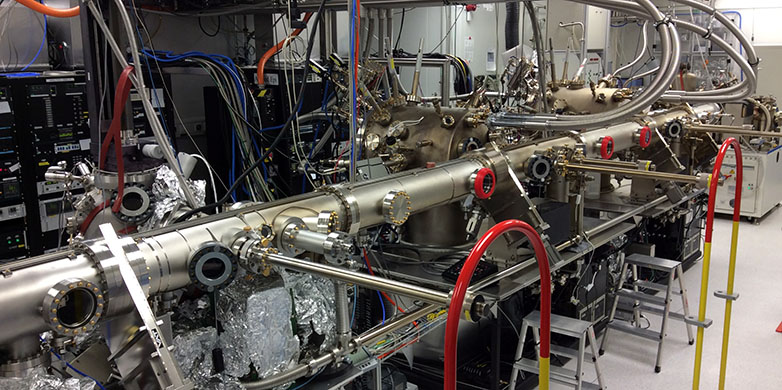
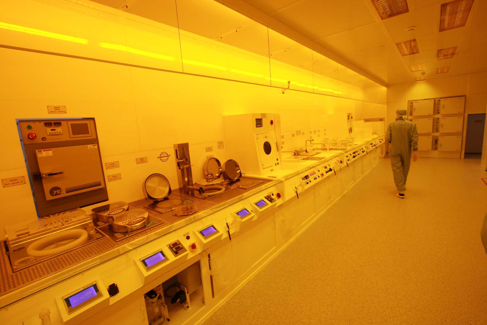
Transistors are fabricated in the FIRST (Frontiers in Research: Space and Time) Laboratory at ETH Zurich, our sophisticated cleanroom facility for advanced Micro- and Nanotechnology. In FIRST we exploit MOCVD and MBE and a full array of semiconductor fabrication tools to realize nanometer scale devices. FIRST-Lab operates a large amount of scientific and technological equipment, ranging from sophisticated epitaxy systems for III-V semiconductors to photo- and nanolithography facilities, numerous vacuum systems for thin film deposition of metals and insulators, dry etching systems, and characterization equipment for the precise analysis of material parameters and processes. Read more
In addition, we also do some experiments in BRNC (Binnig and Rohrer Nanotechnology Center), a cleanroom facility located at IBM Zurich laboratories. BRNC is a multi-user research facility, equipped with state of the art technology and know-how. The cleanroom has class 100 and class 1000 bays with micro- and nanofabrication capabilities. The laboratory serves users from ETH Zurich and IBM. Read more

